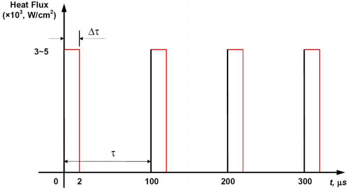
In many communications applications chips operate in a pulsed mode, where rapid temperature transients are continuously experienced within the die. As shown in Figure 1, the chip is turned on for a very short time (~ 2µs) at a very high heat flux (~3 to 5 x 10⁵ W/cm2 right at the gate), causing the temperature to rise rapidly. The temperature decays more slowly during the roughly 98µs that the power is turned off.

Figure 1. High-power communications electronics are typically on for a very short time (~2µs), followed by a much longer recovery time (~100 µs).

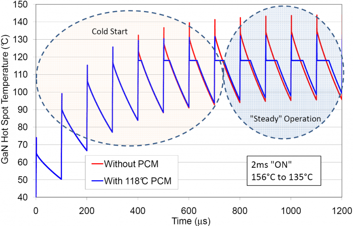
Figure 2: Transient thermal modeling result for GaN device under pulsed operating conditions with and without PCM. The PCM damps the temperature spikes.
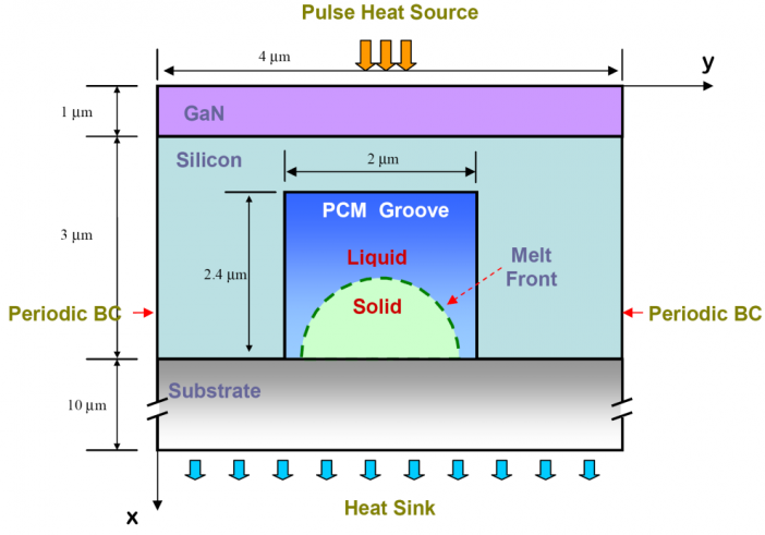
During this rapid cycling, GaN device temperatures without Phase Change Material (PCM) can oscillate between 80°C and 150°C; see Figure 2. The constant thermal cycling and high maximum junction temperatures cause cyclical thermal stresses that lead to reduced reliability. Embedding a Phase Change Material (PCM) in close proximity to the active transistor channels can reduce the peak junction temperature and stabilize the transient temperature profile; see Figure 3. During the heat-generating pulse, the PCM absorbs heat at a constant temperature by melting. During the “off” period the PCM re-freezes at the melting point. The result is a dampened peak temperature experienced by the die, as well as a more constant die temperature throughout the cycle, improving reliability.

Figure 3. GaN chip reliability can be greatly increased by adding PCM very close to the individual gates.
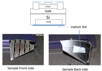
Figure 4. GaN Transistors with PCM-filled grooves.


Figure 5. The normalized drain current remains stable at high pulse width for GaN devices with PCM-filled grooves.
The Phase Change Material (PCM) is located with several µm of the gates and could affect the GaN device behavior. Prior to experimental verification of the concept, a Boltzmann Transport-Based model was used to verify that the PCM-filled grooves would not affect the behavior of the gates.
Prototype devices were fabricated to experimentally test the concept of junction-level thermal storage in devices operated under pulsed conditions. The PCM thermal storage structure was fabricated by etching grooves, and PCM was deposited by melting the PCM into the grooves. The PCM was then encapsulated with a thin indium foil. Figure 4 shows the cross-section of a fully fabricated device, as well a top-view and a bottom-view image of the fabricated chip.
Pulsed current-voltage (I-V) measurements were performed on the devices with PCM-filled grooves and devices without grooves. At each pulse width, the PCM-filled groove measurement was followed by the measurements on devices without grooves, before going to the next pulse width. This procedure allowed for enough time (in the range of minutes) for the re-solidification of the melted PCM. Each data point in Figure 5 represents the maximum drain current at the respective pulse width divided by the overall maximum drain current for a single pulse. As the pulse width decreases, the maximum current through the device increases due to reduced device self-heating. As evident from Figure 5, the maximum current density in the device with PCM material is more stable with the pulse width than in the standard device. The device performance in terms of current density shows a 10% improvement due to enhanced thermal management. This improved performance demonstrates the role of PCM as thermal storage to reduce the temperature increase in the device. It is expected that the performance improvement will be substantially higher after further optimization in terms of groove size and location.


